Looking forward, we believe more disruptive approaches are needed to fundamentally re-think about how we build computers to address von Neumann bottleneck. We envision future computer chips will not solely be made by Si but rather can utilize and optimize the best of various post-CMOS technologies (including but not limited to novel 1D/2D devices, spintronics, resistive switching devices, quantum electrical/optical device, etc.), to effectively complement silicon CMOS in providing auxiliary/ancillary functions (or cost benefits) that otherwise cannot be easily achieved with silicon CMOS. In this research, we take emerging nonvolatile memory technology (e.g., RRAM) as a case study to showcase two general-purpose in-memory computing architectures based on two radically different non-von Neumann machine models. Note that these two architectures are fundamentally different from prior rich literature of applying memory array as domain-specific dot-product computing unit.
Liquid Silicon
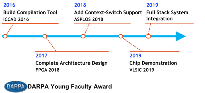
Liquid Silicon (L-Si) is a general-purpose in-memory computing architecture with complete system support that addresses several key fundamental limitations of state-of-the-art reconfigurable data-flow architectures (including FPGA, TPU, CGRA, etc.) in supporting emerging machine learning and big data applications. As compared with most projects in literature which focus on part of the system stack, L-Si is a full stack solution that comprises architecture [Zha2018FPGA], compiler [Zha2016ICCAD], programming model and system integration [Zha2018ASPLOS], with a real chip demonstration Zha2019VLSIC https://penn-cil.github.io/publication/zha-2019-vlsic/. The computing model of L-Si is radically different from state-of-the-art reconfigurable data-flow architectures. It maximally reuses the memory array itself (instead of placing computation units near the array) to perform a) heavy weight computation (logic), b) light weight computation(search), c) data storage (memory), and d) communication (routing), with minimal requirement in CMOS supporting circuitry, which can thus be further placed beneath the array. Therefore, it inherits the great benefits of semiconductor memory in integration density and cost, and offers orders of magnitude more parallel data processing capability in situ in the memory array than the best-known solution today. For the first time, it fundamentally blurs the boundary between computation and storage, by exploiting a continuum of general-purpose in-memory compute capabilities across the whole spectrum, from full memory to full computation, or intermediate states in between (partial memory and partial computation). Thus, it provides programmers (or compiler) more flexibility to customize hardware’s compute and memory resources to better match applications needs for higher performance and energy efficiency. We leverage such unique property and provide compiler support to facilitate the programming of applications written in high-level programming languages (e.g. OpenCL) and frameworks (e.g. TensorFlow, MapReduce) while fully exploiting the unique architectural capability of L-Si. We also provide scalable multi-context architectural support to minimize reconfiguration overhead for assisting virtualization when combined with our system stack.
 Timeline of L-Si project
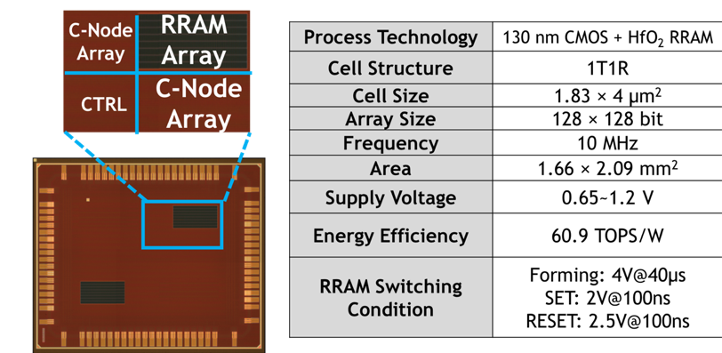
To prove the feasibility of L-Si, we fabricated a test chip in 130 nm CMOS process with HfO2 RRAM – the first real-chip demonstration for general purpose in-memory computing using RRAM.
 Die Photo and Chip Characteristics of L-Si
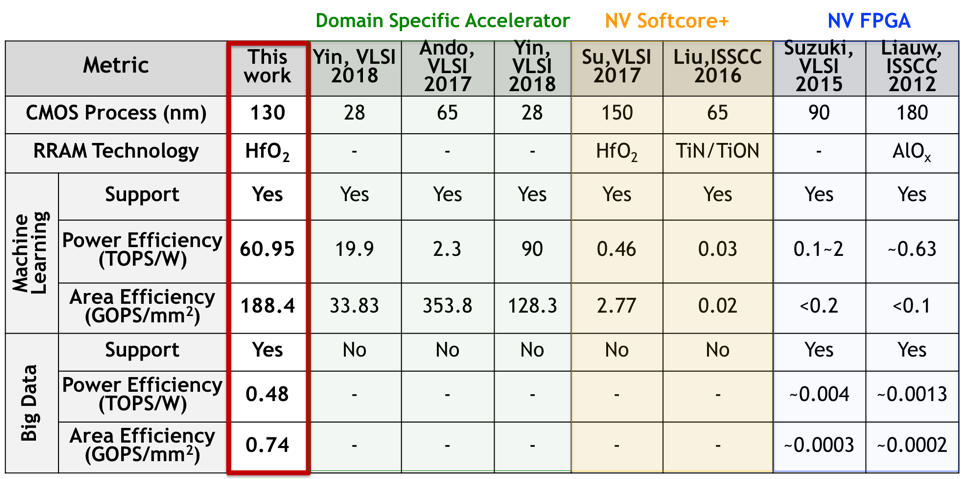
With proposed system support, we evaluated a broad class of legacy and emerging machine learning workloads. Our measurement confirmed the chip operates reliably at low voltage of 650 mV when running these workloads. It achieves 60.9 TOPS/W in performing neural network inferences and 480 GOPS/W in performing high-dimensional similarity search (a key big data application) at nominal voltage supply of 1.2V, showing > 3x and ~100x power efficiency improvement over the state-of-the-art domain-specific CMOS-/RRAM-based accelerators without sacrificing the programmability. In addition, it outperforms the latest nonvolatile FPGA in energy efficiency by > 3x in general compute-intensive applications. As L-Si is a fundamental new computing technology, moving further, we will explore how to scale it up to warehouse computers and scale it down to IoT devices by further specializing the software/hardware stacks.
 Comparing L-Si with State-of-the-Art
Two-Dimensional Associative Processor
The research project, titled “Associative In-Memory Graph Processing Paradigm: Towards Tera-TEPS Graph Traversal In a Box", won the NSF CAREER Award in 2018. In this research, we developed a radically new computing paradigm, namely two-dimensional associative processing (2D AP) to further advance our previous FPGA-based graph processing architectures and fundamentally address their limitations. Mathematically, 2D AP is a new general-purpose computing model that exploits an extra dimension of parallelism (both intra-word and inter-word parallelism) to accelerate computation as compared with traditional AP which only exploit inter-word parallelism. It is particularly beneficial for massive-scale graph processing. For the first time, we provide a theoretical proof that 2D AP is inherently more efficient as measured by “architecturally determined complexity” in runtime/area/energy than both von Neumann architecture and traditional AP paradigm in performing graph computation. We also provide detailed micro-architectures and circuits to best implement the proposed computing model, with domain-special language support. A preliminary published version of 2D AP [Khoram2018CAL] was recognized as best of CAL (IEEE Computer Architecture Letters) in 2018.