Liquid Silicon (L-Si) is a general-purpose in-memory computing architecture with complete system support that addresses several key fundamental limitations of state-of-the-art reconfigurable data-flow architectures (including FPGA, TPU, CGRA, etc.) in supporting emerging machine learning and big data applications. As compared with most projects in literature which focus on part of the system stack, L-Si is a full stack solution that comprises architecture [Zha2018FPGA], compiler [Zha2016ICCAD], programming model and system integration [Zha2018ASPLOS], with a real chip demonstration [Zha2019VLSIC]. The computing model of L-Si is radically different from state-of-the-art reconfigurable data-flow architectures. It maximally reuses the memory array itself (instead of placing computation units near the array) to perform a) heavy weight computation (logic), b) light weight computation(search), c) data storage (memory), and d) communication (routing), with minimal requirement in CMOS supporting circuitry, which can thus be further placed beneath the array. Therefore, it inherits the great benefits of semiconductor memory in integration density and cost, and offers orders of magnitude more parallel data processing capability in situ in the memory array than the best-known solution today. For the first time, it fundamentally blurs the boundary between computation and storage, by exploiting a continuum of general-purpose in-memory compute capabilities across the whole spectrum, from full memory to full computation, or intermediate states in between (partial memory and partial computation). Thus, it provides programmers (or compiler) more flexibility to customize hardware’s compute and memory resources to better match applications needs for higher performance and energy efficiency. We leverage such unique property and provide compiler support to facilitate the programming of applications written in high-level programming languages (e.g. OpenCL) and frameworks (e.g. TensorFlow, MapReduce) while fully exploiting the unique architectural capability of L-Si. We also provide scalable multi-context architectural support to minimize reconfiguration overhead for assisting virtualization when combined with our system stack.
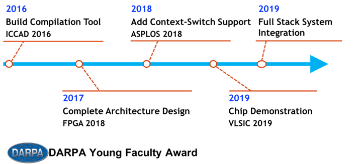
 Timeline of L-Si project
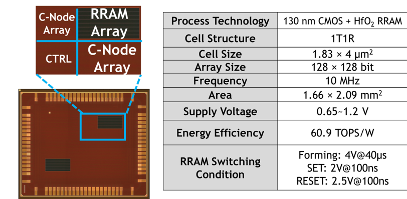
To prove the feasibility of L-Si, we fabricated a test chip in 130 nm CMOS process with HfO2 RRAM – the first real-chip demonstration for general purpose in-memory computing using RRAM.
 Die Photo and Chip Characteristics of L-Si
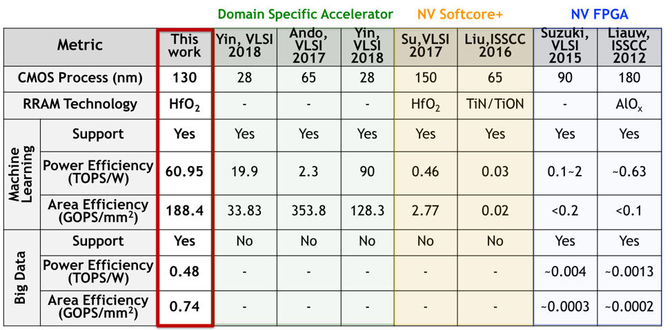
With proposed system support, we evaluated a broad class of legacy and emerging machine learning workloads. Our measurement confirmed the chip operates reliably at low voltage of 650 mV when running these workloads. It achieves 60.9 TOPS/W in performing neural network inferences and 480 GOPS/W in performing high-dimensional similarity search (a key big data application) at nominal voltage supply of 1.2V, showing > 3x and ~100x power efficiency improvement over the state-of-the-art domain-specific CMOS-/RRAM-based accelerators without sacrificing the programmability. In addition, it outperforms the latest nonvolatile FPGA in energy efficiency by > 3x in general compute-intensive applications. As L-Si is a fundamental new computing technology, moving further, we will explore how to scale it up to warehouse computers and scale it down to IoT devices by further specializing the software/hardware stacks.
 Comparing L-Si with State-of-the-Art