Research into noval solutions to complex computing problems
At Penn Computational Intelligence Lab (PennCIL), we are exploring non-conventional computing paradigms beyond Von Neumann computing, to make future computer systems more intelligent, performant, energy efficient, robust, and secure.
We are broadly interested in the big problems in computer system across the full stack. For that, our research spans device, VLSI, design automation, computer architecture and related system support (OS/runtime/compiler/PL), and algorithm. One key differentiator of our research is that besides modeling and simulations, we put strong emphasis on real hardware demonstration through architecting, designing and testing new prototypes, both at chip level and system level to validate our theory. In addition to hardware, we are also interested in bringing up ecosystems and developing key software instrastrucutre to support the new hardware. The systems that we built have achieved several key milestones. One of the highlights is ENIAD, a successor to ENIAC, which is ranked No. 1 on GreenGraph500 list and sets the world record performance in AI-enriched big data analytics (e.g., cognitive search - the next generation search engine). To further extend the system scaling roadmap beyond Moore’s law, we have taped out several new computer chips with complete system support (programming model, runtime, virtualization, API, etc.) that are built with post-CMOS nonvolatile memory technology (e.g., RRAM) integrated with silicon CMOS through monolithic 3D integration, including Liquid Silicon which won DARPA Young Faculty Award (one out of 2 in computer area and one out of 26 across all areas in science and technology nationwide), and Two-Dimensional Associative Processor (2D AP) which won NSF CAREER Award, in addition to the first fabricated in-memory processing chip for search, and a variable-bit storage chip which won IBM’s the highest technical achievement awards, the IBM’s CEO Milestone. More details about our research can be found at Research. A research vision on the importance of interaction between machine learning and computer system can be found at our white paper (co-authored with a number of experts in both machine learning and system fields). A research vision on future memory and storage can be found at our SRC-SIA Webinar Decadal Plan for Semiconductors: New Trajectories for Memory and Storage with Dr. Sean Eilert (Micron), Dr. Carolyn Duran (Intel), Dr. David Pellerin (Amazon), Dr. Steffen Hellmold (Twist Bioscience), Dr. Jesse Mee (Air Force Research Laboratory), moderated by Dr. Heike Riel (IBM). A significant focus of current research is to fundamentally revolutionize computer protection by transforming computer security from being considered an “Art” into a new “Engineering” discipline. Our team is part of a nationwide DARPA-sponsored Security Center, known as CyberSavvy, which is led by Professors André DeHon, Jonathan M. Smith and myself. Please learn more at CyberSavvy.
PennCIL is associated with the nationwide Security Research Center CyberSavvy, the ESE department and the CIS department at the University of Pennsylvania. We were part of Computer Architecture group and Machine Learning group at UW-Madison and part of one of the six SRC JUMP centers - Center for Research on Intelligent Storage and Processing-In-Memory (CRISP).
Our research also greatly benefits from our strong ties with the leading industry and successful technology transfer experience. We would like to thank our sponsors.
Dr. Jing (Jane) Li is the Eduardo D. Glandt Faculty Fellow and Associate Professor (with tenure) at the Department of Electrical and System Engineering (ESE) and the Department of Computer and Information Science (CIS) at the University of Pennsylvania. Dr. Li co-directs the CyberSavvy Research Center, a nationwide security initiative sponsored by DARPA. Previously she was the Dugald C. Jackson Assistant Professor at the University of Wisconsin–Madison and a faculty affiliate with the UW-Madison Computer Architecture group and Machine Learning group. She was one of the PIs in SRC JUMP center – Center for Research on Intelligent Storage and Processing-In-Memory (CRISP). She spent her early career at IBM T. J. Watson Research Center as a Research Staff Member after obtaining her PhD degree from Purdue University in 2009.
She is attracted to all the big problems in computer system across the stack regardless of specific sub-areas. She is especially known for her foundational contributions to memory and memory-driven computing, spanning from device/material to computer architecture, system software and algorithms. She is a passionate computer experimentalist and enjoy building innovative and practical computer systems, both hardware and software. One of her lab’s supercomputer prototypes, ENIAD, ranked No. 1 on the GreenGraph500 list, outperforming many of the most energy-efficient contemporary supercomputers worldwide.
Dr. Li has received numerous awards and honors, including DARPA’s Young Faculty Award (one out of 2 in computer area and one out of 26 across all areas in science and technology nationwide), NSF Career Award, Amazon Faculty Award, and IBM Research Division Outstanding Technical Achievement Award for successfully achieving CEO milestone. She has also received multiple invention achievement awards and high-value patent application award from IBM, as well as the IEEE Benjamin Franklin Key Award for her outstanding achievements in technology transfer. Prof. Li has published over 80 papers in top-tier peer-reviewed conferences and journals and won multiple best paper awards. She has served as an associate editor for IEEE Transactions on Computers, ACM Transactions on Reconfigurable Technology and System, and IEEE Computer Architecture Letter. She holds 46 issued U.S. patents, many of which have been licensed to Fortune 500 high-tech companies. She is a frequently invited speaker and panelist and frequently invited to serve as patent consulting expert by industry. She served on the SRC-SIA Decadal Plan for Semiconductors on Memory and Storage as the only academic representative, joined by prominent industry and government leaders. With over a decade of involvement in the memory industry, she has held various leadership roles such as advisory chair, general chair, and technical chair for the prestigious International Memory Workshop (IMW) – an annual meeting with worldwide memory vendors. She is also an early advocate for establishing Machine Learning System community, serving on the inaugural program committee of the MLsys conference. She serves on many program committees in the broad field of computer engineering, including IEDM, DAC, ISCA, ASPLOS, and others. Presently, she serves as Technical Program Chair for the flagship FPGA Symposium and serves on the ACM/SIGDA Technical Committee on FPGAs and Reconfigurable Computing. Dr. Li is a distinguished member of ACM.
PhD in Computer Engineering, 2009
Purdue University
BSc in Electrical Engineering, 2004
Shanghai Jiaotong University
At PennCIL, our research focuses on future systems in two general directions: 1) Augmenting computer systems with domain specific accelerators and emerging memories, an essential step towards next-generation systems. It requires modest system changes and has low deployment barrier but the performance gain might be potentially limited. 2) Rethinking computer systems with post-CMOS technology, a more aggressive approach in pushing innovations across the entire system stack. It could lead to dramatic improvement in performance but often requires more disruptive change in both hardware and software.
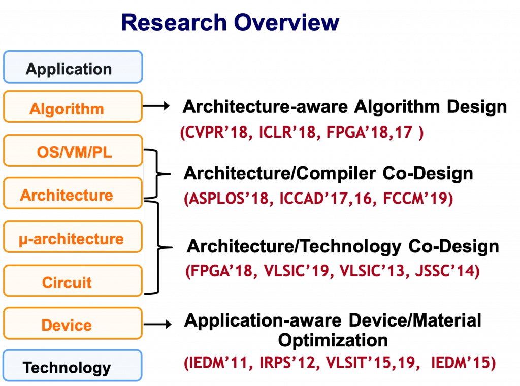
In this research theme, we organize our research around three high-level questions: 1) How to design domain specific accelerators for big data and machine learning applications? 2) What kind of system abstractions are needed to convert hardware specialization into direct benefits that can actually be realized by end-applications and “everyday” programmers? 3) How to effectively evaluate these cross-stack system methods with high fidelity, fairness, and performance? In this research, we aim to answer these questions via the following three paths: 1) architecture/algorithm co-design, 2) mechanisms and abstractions for virtualization, and 3) open-source system research infrastructure.
Extremely large, sparse graphs with billions of nodes and hundreds of billions of edges arise in many important problem domains ranging from social science, bioinformatics, to video content analysis and search engines. In response to the increasingly larger and more diverse graphs, and the critical need of analyzing them, we focus on large scale graph analytics, an essential class of big data analysis, to explore the comprehensive relationship among a vast collection of interconnected entities. However, it is challenging for existing computer systems to process the massive-scale real-world graphs, not only due to their large memory footprint, but also that most graph algorithms entail irregular memory access patterns and a low compute-to-memory access ratio.
In this research, we invented “degree-aware” hardware/software techniques to improve graph processing efficiency. Our research is built atop a key insight that we obtained from architecture-independent algorithm analysis, which has not been revealed in prior work. More specifically, we identified that a key challenge in processing massive-scale graphs is the redundant graph computations caused by the presence of high-degree vertices which not only increase the total amount of computations but also incur unnecessary random data access. To address this challenge, we developed variants of graph processing systems on an FPGA-HMC platform [Zhang2018FPGA-Graph, Khoram2018FPGA, Zhang2017FPGA-BFS]. For the first time, we leverage the inherent graph property i.e. vertex degree to co-optimize algorithm and hardware architecture. In particular, the unique contributions we made include two algorithm optimization techniques: degree-aware adjacency list reordering and degree-aware vertex index sorting. The former reduces the number of redundant graph computations, while the latter creates a strong correlation between vertex index and data access frequency, which can be effectively applied to guide the hardware design. Further, by leveraging the strong correlation between vertex index and data access frequency created by degree-aware vertex index sorting, we developed two platform-dependent hardware optimization techniques, namely degree-aware data placement and degree-aware adjacency list compression. These two techniques together substantially reduce the amount of external memory access. Finally, we completed the full system design on an FPGA-HMC platform to verify the effectiveness of these techniques. Our implementation achieved the highest performance (45.8 billion traversed edges per second) among existing FPGA-based graph processing systems and was ranked No. 1 on GreenGraph500 list.
We have broken our previous record that we made at UW-madison in 2019 and created a new world record at Penn!
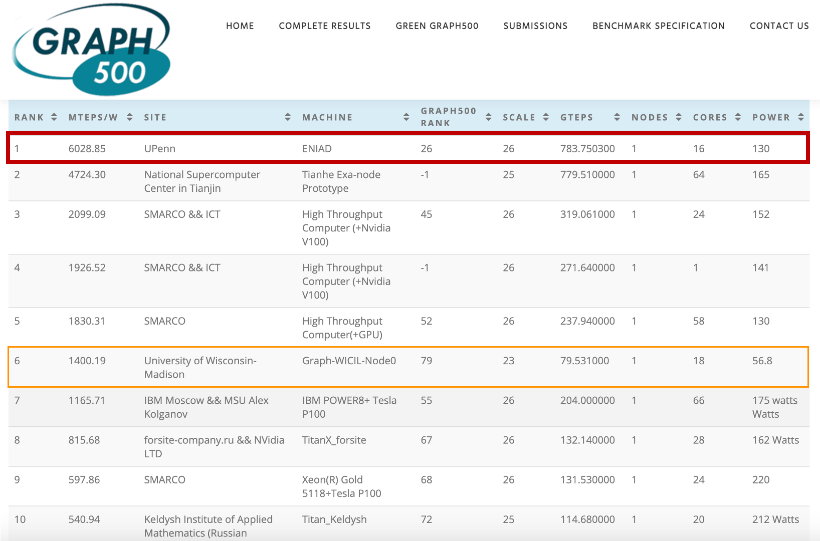 Green Graph500: New ENIAD ranking (updated June 30, 2021)
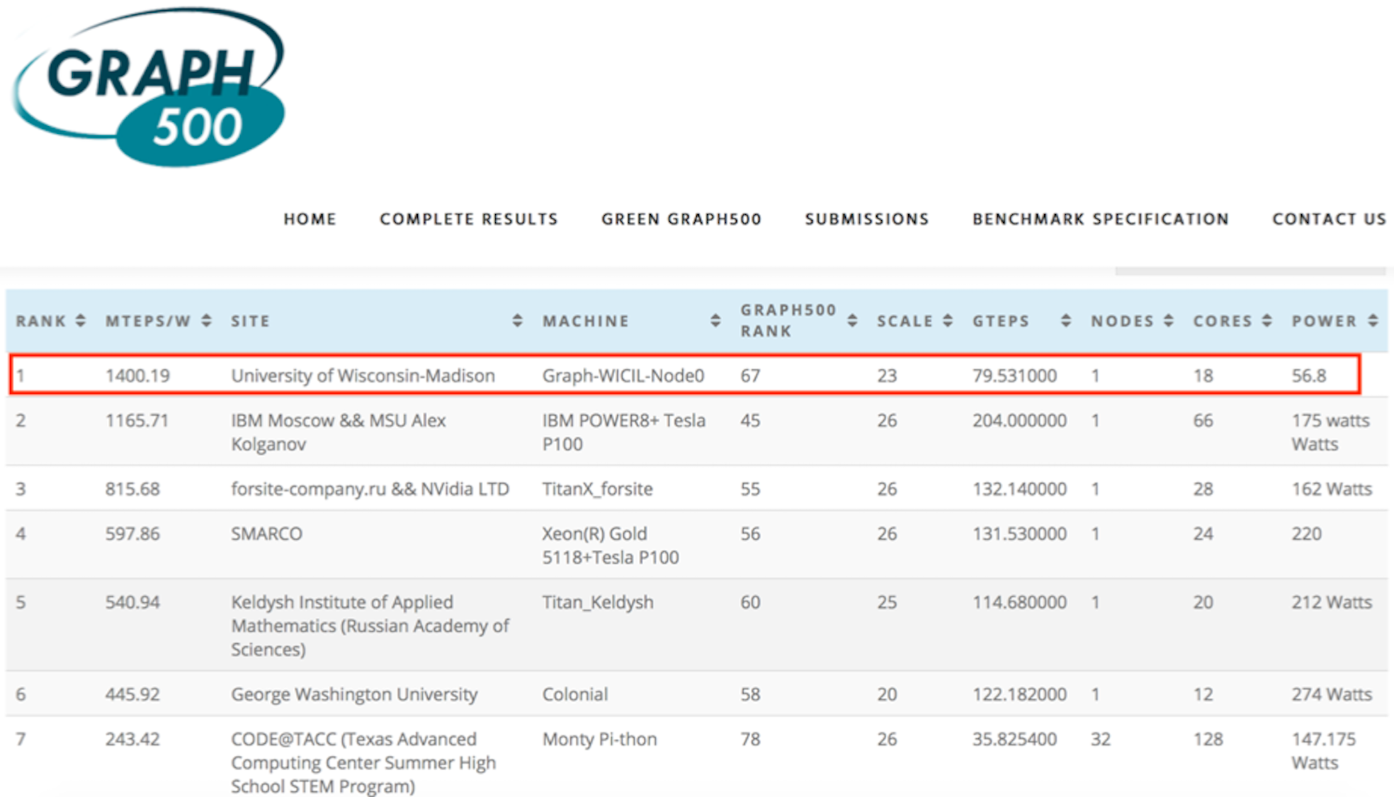 Green Graph500: Old ranking (updated June 19, 2019)
More news can be found at Penn Today, Penn Engineering Today and TCFPGA News.
Deep neural networks (DNNs) deliver impressive results for a variety of challenging tasks in computer vision, speech recognition, and natural language processing, at the cost of higher computational complexity and larger model size. To reduce the load of taxing DNN infrastructures, a number of FPGA-based DNN accelerators have been proposed via new micro-architectures, data ow optimizations, or algorithmic transformation. Due to the extremely large design space, it is challenging to attain good insights on how to design optimal accelerators on a target FPGA.
In this research, we take an alternative, and more principled approach to guide accelerator architecture design and optimization. We borrow the insights from the roofline model and further improve it by taking both on-chip and off-chip memory bandwidth into consideration. We apply the model to quantify the difference between available resources provided by native hardware (FPGA devices) and actual resources demanded by the application (CNN classification kernel). To tackle the problem, we develop a number of hardware/software techniques and implement them on FPGA [Zhang2017FPGA-CNN]. The demonstrated accelerator was recognized as the highest performance and the most energy efficient accelerator for dense convolutional neural network (CNN) compared to the state-of-the-art FPGA-based designs.
While traditionally being used in embedded systems, custom silicon (e.g., FPGAs) has recently begun to make their way into data centers and the cloud (Amazon AWS EC2 F1 instances, Microsoft Brainwave, Google TPU etc.). While these programmable data-flow architectures provide the lucrative benefits of fine-grained parallelism and high flexibility to accelerate a wide spectrum of applications, system support for them in the context of multi-tenant cloud environment, however, is in its infancy and has two major limitations, 1) inefficient resource management due to the tight coupling between compilation and runtime management, and 2) high programming complexity when exploiting scale-out acceleration, for which the root cause is that hardware resources are not virtualized.
In this research, we take FPGA as a case study and develop a full stack solution that can address these limitations and thus, enable virtualization of FPGA clusters in multi-tenant cloud computing environment. Specifically, the key contribution is a new system abstraction that can effectively decouple the compilation and runtime resource management. It allows applications to be compiled offline onto the proposed abstraction and resource allocation to be dynamically determined at runtime. Moreover, it creates an illusion of a single/large virtual FPGA to users, thereby reducing the programming complexity and supporting scale-out acceleration. It also provides virtualization support for the peripheral components (e.g. on-board DRAM, Ethernet), as well as protection and isolation support to ensure a secure execution in multi-tenant cloud environment [Zha2020ASPLOS].
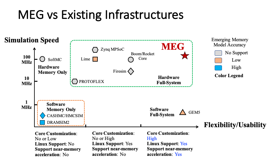
Hardware-software co-design studies targeting next-generation computer systems that are equipped with emerging memories (HBM/HMC, NVM, etc.) are fundamentally hampered by a lack of scalable, performant and accurate simulation platform. Using software simulator is fundamentally bottlenecked by the low simulation speed and low fidelity, making it impractical to run realistic software stack. Such a challenge has limited effective cross-stack innovations (across computer architecture, OS, compiler, machine learning, and domain sciences). Past efforts have largely focused on simulation infrastructure for processor cores with highly simplified models of the memory subsystem. As a key contribution to the community (including SRC JUMP centers, broad academia and industry) to better drive cross-stack memory system research, we have been developing MEG [Zhang2019FCCM] – an open source FPGA- based simulation platform that enables cycle-exact micro-architecture simulation for computer systems with a special focus on memory subsystem (heterogeneous memory, near/in-memory acceleration). In MEG, we combine silicon- proven RTL design of RISC-V cores with configurable heterogeneous memory subsystems (HMC/HBM/NVM). It is capable of running realistic software stacks including booting Linux and comprehensive application software with high fidelity (cycle-exact microarchitectural models derived from synthesizable RTL), flexibility (modifiable to include custom RTL user IP and/or more abstract models), reproducibility, observability, target software support and performance. MEG can be an effective complement to previous RAMP and more recent Firesim projects in covering memory space and a contribution to the open source RISC-V community.
Looking forward, we believe more disruptive approaches are needed to fundamentally re-think about how we build computers to address von Neumann bottleneck. We envision future computer chips will not solely be made by Si but rather can utilize and optimize the best of various post-CMOS technologies (including but not limited to novel 1D/2D devices, spintronics, resistive switching devices, quantum electrical/optical device, etc.), to effectively complement silicon CMOS in providing auxiliary/ancillary functions (or cost benefits) that otherwise cannot be easily achieved with silicon CMOS. In this research, we take emerging nonvolatile memory technology (e.g., RRAM) as a case study to showcase two general-purpose in-memory computing architectures based on two radically different non-von Neumann machine models. Note that these two architectures are fundamentally different from prior rich literature of applying memory array as domain-specific dot-product computing unit.
Liquid Silicon (L-Si) is a general-purpose in-memory computing architecture with complete system support that addresses several key fundamental limitations of state-of-the-art reconfigurable data-flow architectures (including FPGA, TPU, CGRA, etc.) in supporting emerging machine learning and big data applications. As compared with most projects in literature which focus on part of the system stack, L-Si is a full stack solution that comprises architecture [Zha2018FPGA], compiler [Zha2016ICCAD], programming model and system integration [Zha2018ASPLOS], with a real chip demonstration [Zha2019VLSIC]. The computing model of L-Si is radically different from state-of-the-art reconfigurable data-flow architectures. It maximally reuses the memory array itself (instead of placing computation units near the array) to perform a) heavy weight computation (logic), b) light weight computation(search), c) data storage (memory), and d) communication (routing), with minimal requirement in CMOS supporting circuitry, which can thus be further placed beneath the array. Therefore, it inherits the great benefits of semiconductor memory in integration density and cost, and offers orders of magnitude more parallel data processing capability in situ in the memory array than the best-known solution today. For the first time, it fundamentally blurs the boundary between computation and storage, by exploiting a continuum of general-purpose in-memory compute capabilities across the whole spectrum, from full memory to full computation, or intermediate states in between (partial memory and partial computation). Thus, it provides programmers (or compiler) more flexibility to customize hardware’s compute and memory resources to better match applications needs for higher performance and energy efficiency. We leverage such unique property and provide compiler support to facilitate the programming of applications written in high-level programming languages (e.g. OpenCL) and frameworks (e.g. TensorFlow, MapReduce) while fully exploiting the unique architectural capability of L-Si. We also provide scalable multi-context architectural support to minimize reconfiguration overhead for assisting virtualization when combined with our system stack.
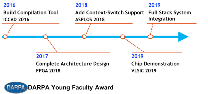 Timeline of L-Si project
To prove the feasibility of L-Si, we fabricated a test chip in 130 nm CMOS process with HfO2 RRAM – the first real-chip demonstration for general purpose in-memory computing using RRAM.
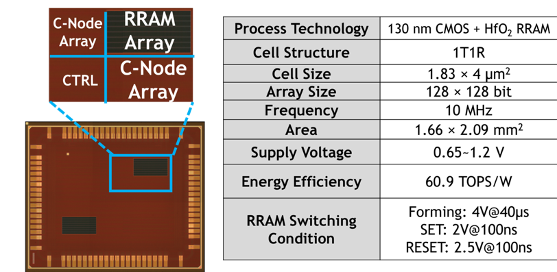 Die Photo and Chip Characteristics of L-Si
With proposed system support, we evaluated a broad class of legacy and emerging machine learning workloads. Our measurement confirmed the chip operates reliably at low voltage of 650 mV when running these workloads. It achieves 60.9 TOPS/W in performing neural network inferences and 480 GOPS/W in performing high-dimensional similarity search (a key big data application) at nominal voltage supply of 1.2V, showing > 3x and ~100x power efficiency improvement over the state-of-the-art domain-specific CMOS-/RRAM-based accelerators without sacrificing the programmability. In addition, it outperforms the latest nonvolatile FPGA in energy efficiency by > 3x in general compute-intensive applications. As L-Si is a fundamental new computing technology, moving further, we will explore how to scale it up to warehouse computers and scale it down to IoT devices by further specializing the software/hardware stacks.
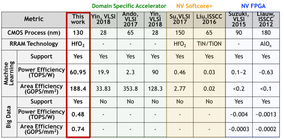 Comparing L-Si with State-of-the-Art
The research project, titled “Associative In-Memory Graph Processing Paradigm: Towards Tera-TEPS Graph Traversal In a Box", won the NSF CAREER Award in 2018. In this research, we developed a radically new computing paradigm, namely two-dimensional associative processing (2D AP) to further advance our previous FPGA-based graph processing architectures and fundamentally address their limitations. Mathematically, 2D AP is a new general-purpose computing model that exploits an extra dimension of parallelism (both intra-word and inter-word parallelism) to accelerate computation as compared with traditional AP which only exploit inter-word parallelism. It is particularly beneficial for massive-scale graph processing. For the first time, we provide a theoretical proof that 2D AP is inherently more efficient as measured by “architecturally determined complexity” in runtime/area/energy than both von Neumann architecture and traditional AP paradigm in performing graph computation. We also provide detailed micro-architectures and circuits to best implement the proposed computing model, with domain-special language support. A preliminary published version of 2D AP [Khoram2018CAL] was recognized as best of CAL (IEEE Computer Architecture Letters) in 2018.